Infusing AI and ML into integrated circuit design for faster chip delivery, better chip performance
This blog post was authored by Jinwook Jung, Jenn Kazda, Derren Dunn, Gi-Joon Nam, Raghu Ganti, Mudhakar Srivatsa, Carlos Costa, and Rama Divakaruni at IBM Research.
As the complexity of modern hardware systems increases, fast and effective design space exploration for better implementations is becoming more difficult to achieve due to higher demand for computational resources. Recent years have seen increasing use of decision intelligence in integrated circuit (IC) design workflows to navigate the design solution space in a more systematic and intelligent manner — aiming to reduce the overall turnaround time and boost the IC design performance.
To address both challenges, we have been working on an AI- and machine learning (ML)-driven IC design orchestration project in order to:
Enable the IC design environment on our hybrid cloud platform so that we can easily scale up or down the workloads according to the computation demands
Produce higher quality of results in shorter total turnaround time
The result is a scalable IC design workload execution that produces higher performance designs by utilizing our AI- and ML-driven automatic parameter tuning capability.
LinkBackground
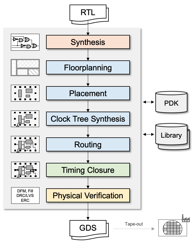
Information on typical digital design flow is shown in Figure 1. It starts from logic synthesis that takes register-transfer-level (RTL) codes and generates a gate-level logic network, called a netlist. The netlist is then transformed into the physical layout through floor planning, placement, clock network synthesis, and routing. We then run timing closure on the final layout for the sign-off timing analysis, and/or fixing the last-minute timing violations. Finally, the physical verification, such as design-rule-correction (DRC) and layout-versus-schematic (LVS) and other required verification checks are done.
In short, the typical digital design flow is a series of transformations and optimizations, consisting of multiple stages. For each stage, there are multiple options for tools to be used. For example, for physical verification, Calibre from the Siemens EDA, or Synopsys ICV or Cadence Pegasus or other open-source design tools can be used. Moreover, each tool provides a variety of its own parameters that determine its behaviors and corresponding optimization results on a given input.
 Figure 1. Digital design flow diagram (adapted from Kahng et al., VLSI Physical Design, Springer, 2011).
The described digital design flow is already complicated with several tools involved (typically from multiple vendors). Each tool has different execution characteristics. For example, placement is a hard-to-parallelize, computation-centric workload, while routing uses a high level of multi-threaded parallelism, and it is virtually impossible to configure on-prem computation resources to satisfy various workload characteristics required by all the relevant tools.
Even worse, during an IC design project, the actual computation demands swing quite significantly and it is extremely difficult to maximize the computation efficiency of on-prem hardware resources during the entire design cycle. Therefore, there is a strong motivation to migrate these IC design workloads to a more cloud-native environment to satisfy dynamic computation demands and maximize resource utilizations on demand.
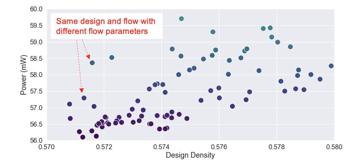
Meanwhile, the design space for a digital IC design is enormous (as exemplified later in Figure 3), and it’s not trivial to find the best graphic design system (GDS) solution for tape-out after multiple stages of optimizations and transformations involving multiple tools. In other words, the optimization focus must be the entire flow, not necessarily individual point tools. The corresponding enlarged design space and causal relationship analysis of required tools in design flows bring about more AI/ML techniques for the best quality of GDS solution.
LinkMigration to cloud-native
Our first step is to containerize the digital design flow. As shown in Figure 1, the design flow involves multiple steps and tools. Each tool in the design flow may require different packages and dependent libraries. So, we created custom container images that can execute various EDA tools used in the design flow. To host large amounts of data we need for IC designs, we also created multiple persistent volumes (PVs) that host PDK, libraries, tools, and user workspaces.
 Figure 2. Containerized design flow execution model on the cloud.
Then, a batch run of the digital design flow optimization is enabled via the containerized flow on the Kubernetes clusters. For cloud resource management and orchestration, HELM is used. Given a user’s flow description in YAML file format, it automatically provisions compute resources across the compute clusters and executes the corresponding design flows. Once the run is completed, the provisioned resources are released to the resource pool.
LinkFinding an optimal digital design
Typically, different designs have different objectives and constraints. For example, some designs may require additional timing optimization, while others may need power reduction optimization. To satisfy such different objectives and constraints, EDA tools provide so-called parameters that change optimization tool behaviors. For example, we can guide the tools to spend more time searching for better logical structure, or we may want to have tools to do better power optimization. We can achieve these different behaviors by setting different values on the provided parameters of the tools.
However, the problem is that such a parameter space is large: hundreds or even thousands of parameters affect the design outcome, and it is a non-trivial task to find an optimal parameter setting that satisfies specific design objectives and constraints for a given design.
 Figure 3. Design space exploration example.
Figure 3 illustrates the difficulty of the flow parameter tuning problem. It shows all the different design results obtained by setting different parameter values. The X-axis is the design density and Y-axis is the power consumption. Both are important quality metrics of a given design. We observe that, given the same design density, the power consumption can vary quite significantly. Similarly, for the iso-power consumption, the design density can swing enormously.
LinkAI for optimal digital design
To tackle this problem, we developed an ML-driven automatic flow tuner. The tuner sees the design flow as a black box, while providing a generic interface to apply parameters to the flow and compute corresponding reward values from the results. With such a generic interface, our flow tuner is applicable to arbitrary design flows. Furthermore, it provides a flexible user interface, where users can specify the preferred search algorithm, resource constraints, and tunable parameters. As shown in the pseudo code from Figure 4, it is an iterative parameter search engine. At each iteration, it creates a new parameter setting guided by ML algorithms, executes the design flow, and calculates the reward value. Once the parameter search is done, it returns the best result it found thus far.
 Figure 4. AI/ML-based design flow tuner.
 Figure 5. Containerized AI/ML-based design flow tuning with Ray.
Figure 5 shows the extended containerized design flow with the AI/ML-based flow tuning capability. We leverage the open-source project Ray and specifically Ray Tune to identify the optimal design. It naturally supports scalable and distributable executions of the automatic Flow Tuner by seamlessly integrating and scaling complex AI/ML pipelines in a cloud-native manner.
Now, for some interesting evidence that our design Flow Tuner works:
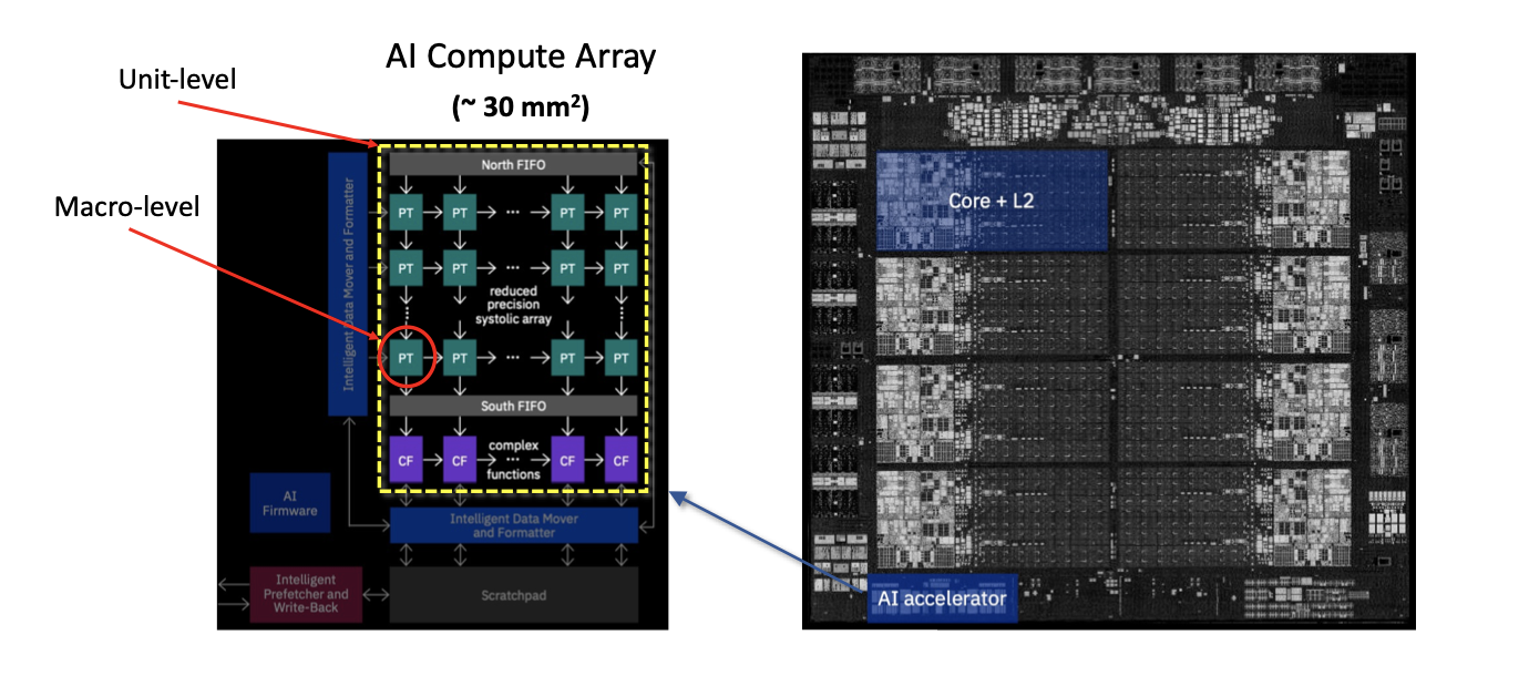
We applied our Flow Tuner to the on-chip AI accelerator design that was included in IBM’s signature Telum microprocessor (Figure 6). Basically, the team took the AI Compute Array design, which is a ~30 mm2 application-specific integrated circuit (ASIC) design, and demonstrated that the cloud-based containerized design flow can build that size and complexity of an ASIC chip on the IBM Cloud, using commercial design tools and technology. Leveraging the Flow Tuner, the team was able to improve the quality of results of the design quite significantly.
 Figure 6. IBM Telum processor with on-chip AI accelerator.
Then, we also applied it to an IBM internal design. For this experiment, we took an expert designer’s already-optimized design as a baseline. The timing of the design is closed, so the tuning objective was to minimize the power consumption of the design. The first plot in Figure 7 shows the power savings that could be made by an expert designer manually: 0.82%, 1.21%, and 2.56% per iteration. Then, the third iteration result is fed into the automatic parameter tuner with the objective of power minimization, and our Flow Tuner was able to reduce the power consumption by an additional 8.93% by running automatic iterations.
The right plot shows the tuning iterations. We observe that as the iteration proceeds, the tuner improves the power consumption gradually and returns the final best result.
 Figure 7. Design flow tuning results for power optimization.
LinkConclusion
In summary, we demonstrate that we can build a cloud-based IC design environment, including the containerized digital design flow, on Kubernetes clusters. We extended the containerized design flow with the automatic parameter tuning capability using AI/ML techniques. Finally, we demonstrated that the automatic parameter tuning can be executed in a more scalable and distributable manner using the Ray platform.
IBM contributes to Ray through Project CodeFlare.
Interested in learning more? The IBM Research team will be presenting at the June 22 Ray Meetup. Register here.


